Mini-lens technology is revolutionizing the world of optics and electronics, paving the way for a new era of consumer devices. Developed in the Capasso lab at Harvard, these innovative lenses utilize metasurfaces crafted from tiny pillars to manipulate light efficiently, all while maintaining a compact design. Rob Devlin, a key figure in the creation of mini-lens technology, now leads the startup Metalenz, which produces millions of these advanced components for various consumer electronics. As laptops, smartphones, and tablets demand more intricate features, the significance of mini-lenses becomes more apparent, offering solutions that traditional optics couldn’t achieve. With the ongoing integration into products like the iPad and Google’s Pixel 8 Pro, mini-lens technology is poised to disrupt industries and redefine how we use optical systems in everyday life.
The emergence of micro-lens technology represents a significant shift in the field of optical devices, bringing about innovative solutions for modern electronics. Often referred to as optical metasurfaces, these miniature lenses are designed using a unique technique involving precisely engineered nano-structures that manipulate light with high precision. Rob Devlin, who played a pivotal role in developing this technology at Harvard, has since founded a startup dedicated to mass-producing these cutting-edge lenses for the consumer market. As the demand for sleeker and more advanced consumer electronics rises, the relevance of micro-lens technology grows, promising to enhance functionalities in everything from smartphones to cameras. This pioneering approach serves not only to minimize size but also to expand the capabilities of optical systems significantly, marking a transformative leap in the electronics industry.
Innovations in Metalens Technology
Metalens technology has revolutionized the optics industry by introducing flat, ultrathin lenses that outperform traditional curved glass lenses in many applications. These innovative designs utilize metasurfaces—structures engineered at the nanoscale—to manipulate light in unprecedented ways. This shift towards flat optics not only simplifies the design process for consumer electronics but also opens up new possibilities in compact device form factors, which are crucial in today’s market where space is a premium.
The significant advantages brought forth by metalens technology include reduced weight and size, which directly address the challenges posed by conventional optics in smartphones, tablets, and cameras. As manufacturers strive to integrate advanced features while maintaining sleek designs, metalenses present an ideal solution by enabling optical functionalities in thinner, lighter packages. Moreover, with the advances made by startups like Metalenz, the efficiency of producing these lenses has improved, paving the way for their widespread adoption.
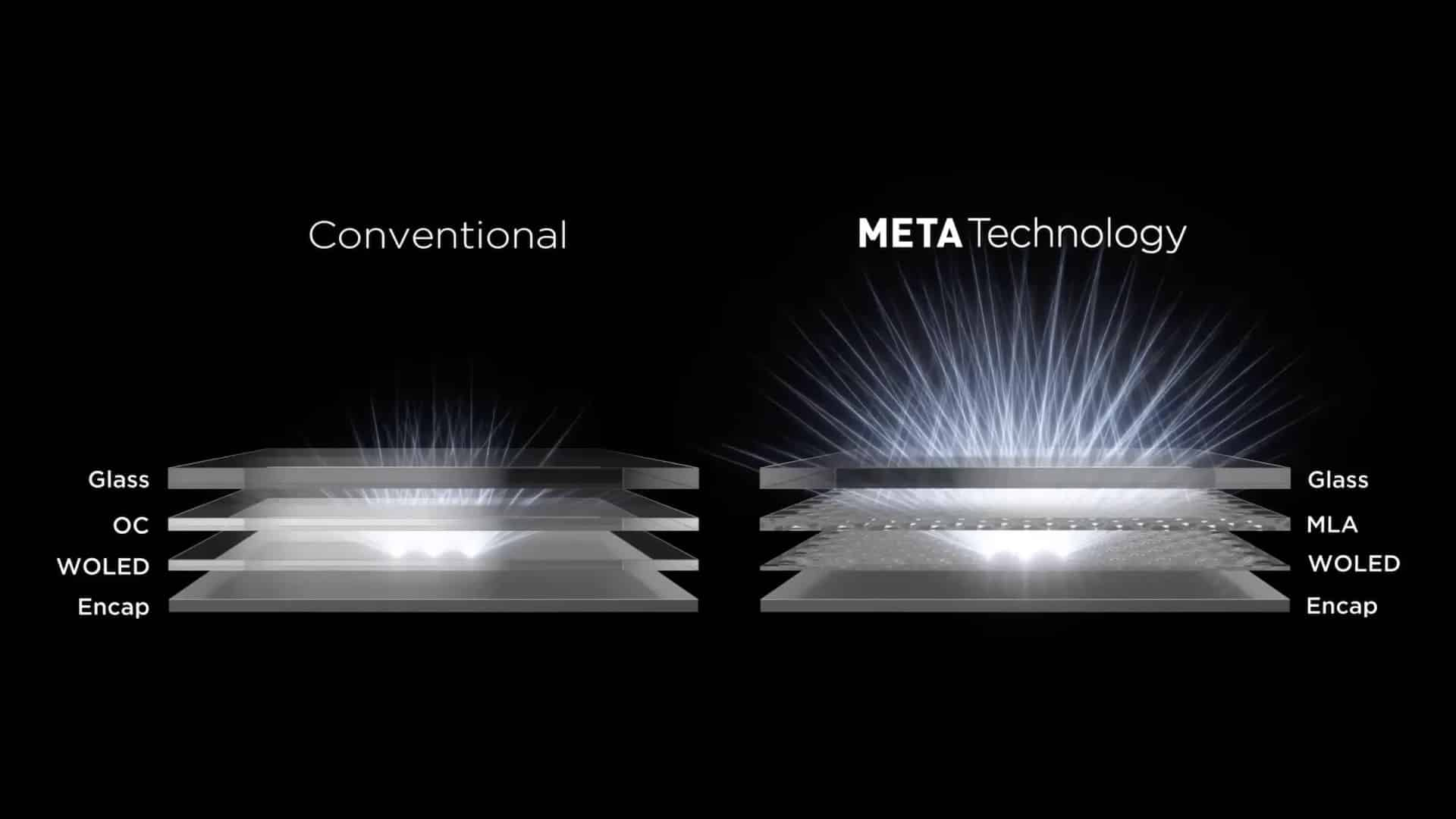
The Role of Metasurfaces in Modern Electronics
Metasurfaces, the cornerstone of metalens technology, are composed of thousands of sub-wavelength structures that interact with light in a highly sophisticated manner. This capability allows for precise control over light propagation, resulting in better imaging capabilities and functions such as advanced 3D sensing, which are increasingly vital in consumer electronics. Companies like Metalenz leverage these properties to enhance their products, enabling features like facial recognition and augmented reality that rely on accurate depth perception.
As the demand for advanced functionalities in smartphones continues to rise, metasurfaces are proving to be invaluable. They not only help in shrinking the size of essential components but also reduce manufacturing costs, making technology more accessible for a wider range of devices. The effective integration of metasurfaces can lead to improved performance in a variety of applications across the tech industry, placing pressure on competitors to innovate or risk lagging behind.
Rob Devlin and the Rise of Metalenz
Rob Devlin, a pivotal figure in the creation of metalens technology, has transformed his academic research into a thriving startup, Metalenz. Under his leadership, the company has transitioned from a lab prototype to mass production within a remarkably short timeframe. This success story underscores the powerful synergy between academic research and entrepreneurial innovation, illustrating how university-backed startups can lead to groundbreaking advancements in technology.
Metalenz exemplifies this dynamic as it scales up its production of metasurfaces to meet the growing demands of consumer electronics. By focusing on collaborations with other tech companies and leveraging the cutting-edge research from the Capasso lab at Harvard, Devlin aims to push the boundaries of what is possible with optics in everyday devices. The continual refinement of metalens technology not only enhances existing applications but also drives the development of new functionalities, ensuring that Metalenz remains at the forefront of the optical revolution.
Unique Applications of Polarization Cameras
Metalenz’s innovations extend into the realm of polarization cameras, a crucial tool in areas such as security and healthcare. Traditional polarization cameras are bulky and expensive, but with the introduction of Metalenz’s minisaturization techniques, these cameras can now be produced at a fraction of the size and cost. This advancement allows for broader adoption in consumer devices, paving the way for enhanced security features, including identification systems that utilize unique polarization signatures.
Furthermore, polarization information has far-reaching applications beyond consumer electronics. It can be employed in crucial medical diagnostics, such as distinguishing between healthy and cancerous tissues based on their polarization signatures. Additionally, this technology has potential in environmental monitoring, providing vital data regarding air quality and pollution levels. The versatility of polarization cameras enabled by metasurfaces marks a significant leap in technology that could transform various sectors.
Future Innovations in Consumer Tech
Looking ahead, the integration of metalens technology into consumer electronics is set to expand dramatically. With companies focusing on maximizing the capabilities of these devices, the potential for creating even more compact and efficient products is enormous. Upcoming devices may feature enhanced imaging technologies specifically designed for features such as augmented reality (AR) and virtual reality (VR), which rely heavily on high-quality optics.
As Metalenz continues to innovate, the company is not only enhancing existing technologies but is also exploring entirely new functionalities. The interplay between optics and digital experiences promises to shape the future of consumer technology in remarkable ways, bringing sophisticated capabilities to everyday devices even further.
The Impact of Startups on Technological Advancements
Startups like Metalenz play a crucial role in driving technological advancements by bringing groundbreaking ideas from research to market. The agility and innovative spirit of these smaller companies allow them to disrupt established industries, offering fresh solutions that address existing challenges. By focusing on maximizing research outcomes, startups contribute significantly to the evolution of sectors such as consumer electronics, enabling the development of more efficient and affordable technologies.
Moreover, these startups often build upon the foundations laid by academic institutions, establishing collaborations that not only foster innovation but also ensure that cutting-edge research translates into practical applications. As Metalenz demonstrates, when entrepreneurial ambition meets academic rigor, the results can transform industries and create entirely new markets.
Collaboration Between Academia and Industry
The close collaboration between academia and industry is vital for advancing technologies like metasurfaces and metalenses. This partnership often allows for the rapid application of theoretical research, propelling innovations into commercial products faster than traditional models of product development. Companies like Metalenz are leveraging this synergy to harness the full potential of university research, incorporating insights from scholars like Federico Capasso into their product development processes.
Such collaborations not only help startups navigate early-stage challenges but also accelerate their growth trajectories. As proven by the success of Metalenz, the ability to draw from both academic insight and industry experience allows for the successful navigation of the complex landscape of technology commercialization. This model showcases the critical importance of nurturing environments where academia and industry can work synergistically.
Challenges on the Horizon for Metalenz
Despite its successes, Metalenz faces a competitive landscape filled with emerging technologies and companies aiming to replicate its success. The rapid advances in fields such as artificial intelligence and machine learning can pose challenges, as they offer alternative solutions to the problems Metalenz aims to address with its optical innovations. Players in the tech industry are continuously vying for dominance in the market, making it essential for Metalenz to innovate consistently.
To overcome these challenges, the company plans to focus on further enhancing its existing product lines while exploring new applications for its technology. By remaining adaptable and committed to research and development, Metalenz hopes to stay ahead of competitors and continuously meet the demands of an ever-evolving tech landscape. Fostering relationships with academic institutions further bolsters this endeavor, ensuring that they remain at the forefront of optical innovation.
The Future of Light Manipulation Technologies
The future of light manipulation technologies promises exciting developments, especially with advancements in metasurfaces. As researchers continue to push the boundaries of how light is controlled at the nanoscale, we can expect to see more sophisticated applications emerging across various fields, from consumer electronics to healthcare. Innovations in mini-lens technology provide new ways to enhance optical functionalities in everyday devices, which is crucial as we move towards more immersive digital experiences.
Looking ahead, ongoing research and development efforts in this domain are likely to yield groundbreaking inventions that utilize light in transformative ways. The convergence of optics and technology will be fundamental in shaping how we interact with the digital world, heralding a new era of smart devices that seamlessly integrate advanced optical capabilities into their design.
Frequently Asked Questions
What is mini-lens technology and how does it relate to metasurfaces?
Mini-lens technology refers to a new type of lens developed using metasurfaces, which are engineered surfaces that manipulate light at the nanoscale. This technology allows for the creation of lenses that are significantly smaller, cheaper, and more efficient than traditional lenses made from glass or plastic. By utilizing tiny pillars on a wafer, mini-lenses can focus light similarly to conventional lenses, making them ideal for various consumer electronics.
How is Metalenz utilizing mini-lens technology in consumer electronics?
Metalenz is a startup leading the commercial production of mini-lenses, specifically light-focusing metasurfaces, for consumer electronics. These innovative lenses are integrated into popular devices, enhancing features like camera performance, 3D sensing, and augmented reality. By producing millions of these metasurfaces, Metalenz is transforming traditional optics and enabling manufacturers to design slimmer and more advanced electronic devices.
What are the advantages of using mini-lens technology over traditional optics?
The advantages of mini-lens technology, particularly through the use of metasurfaces, include reduced size, lower production costs, and the ability to mass-produce lenses at scale. This technology enables the integration of advanced optical features into compact devices without the bulk of traditional glass lenses, thus fostering innovation in the design of smartphones, tablets, and more.
What role does Rob Devlin play in the development of mini-lens technology?
Rob Devlin is the CEO of Metalenz and played a crucial role in developing mini-lens technology during his Ph.D. studies at Harvard. His work focused on refining metasurfaces and ensuring they could be mass-produced for the consumer electronics market. Under his leadership, Metalenz has successfully brought innovative optical solutions to a variety of applications, including facial recognition and augmented reality.
How does the mini-lens technology from Metalenz enhance camera capabilities?
The mini-lens technology from Metalenz improves camera capabilities by incorporating metasurfaces that can focus light more efficiently than traditional lenses. This results in slimmer camera modules that can maintain high image quality while enabling additional features, such as 3D sensing and depth detection, which are essential for augmented reality and enhancing user experiences in consumer electronics.
How can mini-lens technology impact device security with Polar ID?
Metalenz’s mini-lens technology is set to enhance device security through Polar ID, which uses light polarization to identify unique characteristics of users. Unlike traditional methods, this technology allows devices to detect a person’s polarization signature, making it much harder to spoof with a 3D mask, thereby providing a new layer of security for smartphones and other devices.
In what other applications can mini-lens technology and polarization metasurfaces be used?
Beyond consumer electronics, mini-lens technology and polarization metasurfaces can be applied in various fields, including medical diagnostics to detect skin cancer by analyzing polarization signatures of skin, environmental monitoring for air quality assessment, and improved imaging systems that require compact lens solutions. The versatility of this technology enables advancements across many sectors.
What was the historical significance of mini-lens technology development at Harvard?
The mini-lens technology’s development at Harvard, particularly in the Capasso lab, represents a significant shift in optical engineering. This innovative work led to the establishment of Metalenz and propelled research into mass-market applications that disrupt traditional lens manufacturing. The journey from lab research to commercial product has helped foster a new industry that combines academic insights with real-world technology solutions.
| Key Point | Description |
|---|---|
| Introduction of Mini-Lens Technology | Rob Devlin, a graduate from Harvard, developed innovative mini-lenses during his studies, which now have applications in consumer electronics. |
| Mass Production | Metalenz reported production of around 100 million light-focusing metasurfaces that are integrated into popular devices. |
| Functionality | These mini-lenses use a series of tiny pillars on a thin wafer to bend light, making them smaller and cheaper compared to traditional lenses. |
| Industry Impact | It is transforming the optical industry, paving the way for new applications in consumer electronics. |
| Future Developments | Metalenz aims to innovate further with developments like Polar ID, a technology enhancing device security and functionality. |
Summary
Mini-lens technology represents a significant breakthrough in optics, having evolved from laboratory research to mass application in consumer devices. Initiated in the Capasso lab at Harvard and commercialized by Metalenz, mini-lenses are revolutionizing the way light is manipulated in electronics. The strategic advancements highlight not only the progress in manufacturing but also the potential for diverse applications in security and health monitoring. As this technology continues to evolve, it opens new avenues for innovation, ensuring mini-lens technology remains at the forefront of optical development.